
AMATTSM
AMAT: Structural Capital Intensity Shift to Materials Engineering
FUNDA
TSMC N2 GAA and 2027 BSPDN add process steps; AMAT's TSMC rev +20-30% in 2026, faster in 2027.
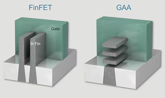
Our positive stance on Applied Materials (AMAT) is predicated on a fundamental divergence in semiconductor manufacturing physics. For the past decade, lithography has been the primary driver of wafer cost. However, as the industry transitions to 2nm Gate-All-Around (GAA) and Backside Power Delivery Networks (BSPDN), the primary scaling bottleneck shifts from “printing smaller lines” to “building complex 3D structures” and “engineering new materials.”
This architectural shift triggers a structural increase in capital intensity for Deposition (PVD/CVD/ALD) and Removal (CMP/Etch). Applied Materials, with its breadth of portfolio and dominance in integrated vacuum platforms, is the primary beneficiary of this transition.
Our latest supply chain investigation indicates an accelerating revenue trajectory from TSMC. AMAT’s revenue contribution from TSMC to grow 20-30% YoY in 2026 , with momentum expected to accelerate even further in 2027. This ramp is underpinned by the simultaneous high-volume manufacturing adoption of GAA and the subsequent deployment of BSPDN, which disproportionately benefits AMAT’s specific product portfolio compared to prior FinFET generations.
The 2026 Inflection: TSMC N2 Ramp
The growth in 2026 corresponds to the volume ramp of TSMC’s N2 node. Unlike the transition from N5 to N3, which was a FinFET shrink, N2 introduces GAA transistor. This architecture requires the deposition of alternating Si/SiGe layers and significantly more complex Gate Metal stacks. This drives immediate demand for AMAT’s Epi and CMP tools, as planarization steps increase by an estimated 20-30% to manage the topography of the new gate structure.
Continue reading with FUNDA
This report is available to subscribers. Sign in or subscribe to read the full analysis.